(Auto-Translation via LLM)
The Taalas HC1 has recently attracted widespread attention. This article attempts to decode its architecture from a technical perspective to serve as a reference for industry peers. The analysis is based on published patents and interviews from Taalas. Because its architecture has not been made public, many details require reverse engineering and speculation, so accuracy cannot be guaranteed.
The HC1 features two major architectural advancements:
- It upgrades the naive matrix multiplier to a mechanism specifically tailored for quantized operations, eliminating redundant calculations. The computing mechanism can be summarized as “Multiply-Select-Add” (rather than the standard “Multiply-Add”).
- It uses ROM as the storage medium for model weights, achieving very high density. Modifying the model weights only requires altering two upper-layer via masks.
The new computing mechanism improves efficiency by leveraging quantization effects, rather than the constant nature brought about by fixed weights. Therefore, a very clear boundary still exists between memory and computation in the HC1 architecture. This means the act of memory access during HC1’s operation is still present; only the accessed target has changed. In terms of density, this solution is already excellent; however, the current computing mechanism has not yet fully utilized the constancy of the weights, leaving further room for exploration in terms of energy efficiency. Its weights need to be read from the ROM row by row, which limits peak performance capabilities.
In the context of linear algebra, every real-valued quantity can take continuous values; but in computers, numerical precision is always limited. Especially after quantizing and compressing a model, quantization effects become far more prominent. For example, if every quantity in a weight matrix is quantized to a 2-bit representation, regardless of how the number system is designed, each number can only take a maximum of 4 different values. Under a binary integer system, these 4 values are 0, 1, 2, and 3. These four specific values can be arbitrarily designed to form number systems other than binary to help quantize more accurately, but there are at most four, which is strictly limited by the information capacity of two bits. Therefore, without loss of generality, this article assumes the values are
When an input neuron activation value is to be multiplied with such a weight matrix, because the number of operations exceeds the number of value types, the operations inevitably generate a massive amount of repetition. For example, assuming the first column of the weight matrix is
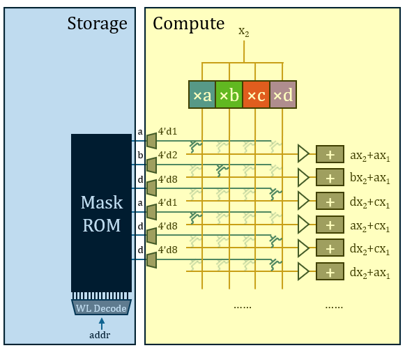
To address how to eliminate this repetition to save hardware overhead, academia has proposed various solutions. The strategy adopted by Taalas is the LUT (Look-Up Table) scheme, which eliminates repeated multiplications through pre-computation and selection. Since the weight value space is extremely small after quantization, the products of the input activation value and all possible weight values can be entirely pre-computed once, listing all potentially used products. Every subsequent individual multiplication operation can then be replaced by selecting a ready-made value from the pre-computed results. Reviewing the 14 patents published by Taalas, its core mechanism is primarily documented in Large parameter set computation accelerator… (US20250123802A1).
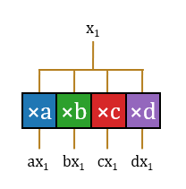
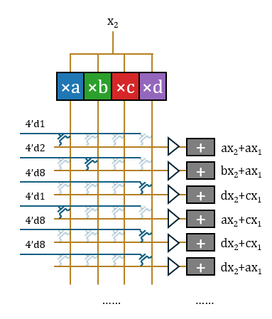
- Multiply: First, pre-computation is performed, multiplying
with the constants , , , and respectively. Every input neuron activation value will be pre-multiplied with all possible weight values. To further compress the area, the operations do not need to be completed in parallel. can be input bit-by-bit from LSB to MSB, and the multiplication with fixed values consists of delays (DFF) and carry-save adders (CSA). All signal lines can be simplified to a single bit. The output signal lines are extended to form a parallel bus structure for selection in subsequent steps.
- Select: Thus, the operation of
with the vector becomes a selection. 16 horizontal signal lines are set up to carry the operation results, forming a crossbar switch with the pre-computation output signal lines. Each horizontal line needs to form a connection at the intersection corresponding to the vector value to extract the required pre-computed signal. Since 16 items are too many, the latter part is omitted in the illustration; its structure is repetitive.
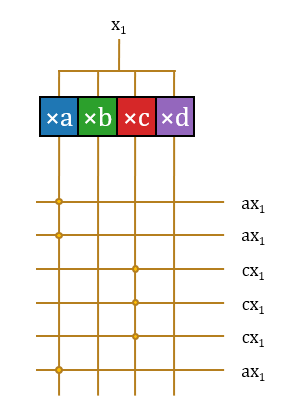
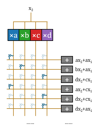
- Add: At this point, the structure has completed these 16 operations without repetition. These operations belong to 16 different output neuron activation values, thus requiring 16 different accumulators to accumulate them.
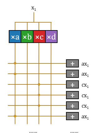
In this way, the structure completes the multiplication of an input scalar
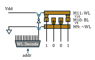
Usually, using PTL to construct transmission gates requires a pair of transistors, but using a single transistor here is reasonable. A single transistor will only cause a threshold voltage drop; adding a Buf outside the crossbar switch array and before the accumulator to restore the signal is sufficient. Bajic claimed the company hand-drew a portion of the layout, which is very likely for handling this specific part.
The gate of the transistor needs to be provided with a one-hot control vector, which can be read directly from the ROM. Thus, the complete matrix operation architecture is essentially formed. Surrounded by auxiliary functions like vocabulary lookup tables, random sampling, normalization, softmax, positional encoding, and activation functions, paired with a medium-capacity SRAM for storing KV (the model’s own context is very short), the entire model is fully implemented.
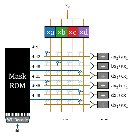
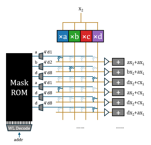
Converting each 2-bit weight to a 4-bit one-hot encoding and writing it to ROM requires a relatively large ROM capacity, which contradicts the “store four bits away” claim (HC1 claims to use 3/6-bit mixed quantization; if it were a one-hot representation, it should “store eight bits” at least). Therefore, I believe what is burned into the ROM should be the original weight values, which are then converted to one-hot via a 3-to-8 decoder. The decoder is a one-dimensional structure outside the matrix, and its total overhead is not significant.
Taalas claims that customizing the Mask ROM requires changing two layers of photomasks. This is highly likely for two layers of vias, whose structure should be as illustrated: VDD and GND controlled by wordlines complementarily fill the upper and lower layers of Trenches. The middle Trench serves as the bitline for reading out, and vias are placed above or below the bitline in a complementary manner to represent 0 or 1.
Therefore, the truly hardwired part in Taalas’s scheme is only the vias of the ROM. The entire architecture can still be clearly divided into a storage part and a computing part; memory and computation are structurally separated. It does not eliminate memory access in a broad sense, but merely changes the medium of the accessed target from SRAM (Groq) or HBM (Nvidia) to ROM, and the accessed data is also highly likely to be unprocessed original weight values. If accessing memory on the same chip is not considered memory access, then the goal of eliminating this narrow “off-chip memory access” has actually already been achieved by the Groq architecture.
The computing part is a classic quantized computing architecture, very similar to UNPU, Cambricon-P, etc. Utilizing these architectures to improve the efficiency of quantized matrix multiplication does not require assuming the weights are fixed. I have provided an architecture diagram comparison for reference.
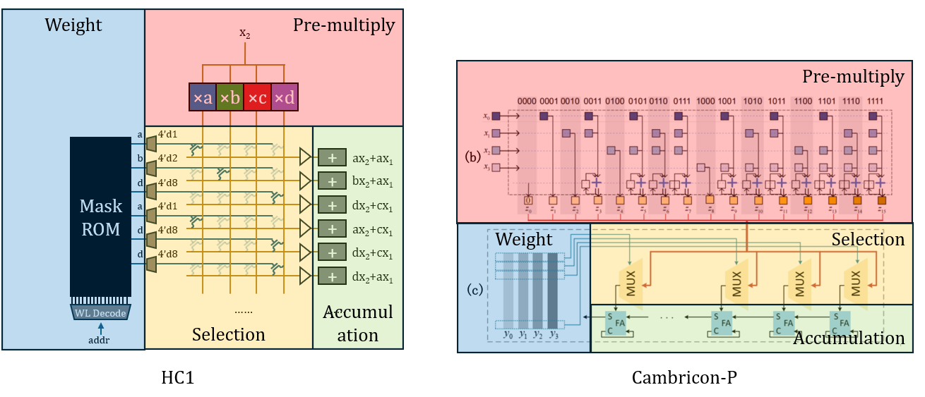
Under this architecture, because structures like pre-multiplication, accumulation, decoders, and Bufs are all located at the periphery of the array and are one-dimensional structures, they can all be regarded as preparatory or finishing work for the actual computation. Only the two-dimensional crossbar switch is regarded as the true computation. From this perspective, the statement “a single transistor completes all operations” also makes some sense, though slightly exaggerated. From a stricter perspective, it only undertakes the selection/gating function in the operation.
The computing part can also be directly used to process variable-value matrices, as long as the source of the crossbar switch array control signal is switched from ROM to SRAM. I suspect this is how HC1 supports LoRA. This architecture can achieve an area balance between computing devices (mainly limited by transistor components) and memory devices (mainly limited by high-level metal vias) by adjusting size parameters. However, the computation needs to be completed by reading the ROM row by row, so processing a complete matrix requires traversing all addresses of the entire ROM, which limits the peak computing power. If multiple matrices are written into the same ROM, it becomes very difficult for this architecture to implement pipeline parallelism.
In terms of density, since computation and ROM storage are separated, the ratio can be adjusted freely, so the area is mainly limited by the ROM. Assuming the Half Pitch of the vias used for ROM encoding is 62 nm, and the ROM bit-cell density is 0.015 μm², an 8B model with an average of 4.0 bpw would require 480 mm², which basically matches the implementation. If the layers are reduced to 38 nm, the density becomes 0.0058 μm², and the model would only need about 180 mm², but it cannot be completed in a single exposure, so the model update cost would double. Since hardwired chips usually do not require ultra-large-scale mass production, if it can be coordinated with the manufacturing process to introduce e-beam lithography in the production line to achieve maskless via processing, it will help realize high-density variable vias at a low cost. Imagine that changing models for chips no longer requires redesigning; merely introducing one or two layers of e-beam drilling processes costing a few thousand yuan per wafer could continuously output chips equipped with various models. The final cost barrier for the commercialization of hardwired language processors would be resolved.
Strictly from an architectural design perspective, the HC1 still has many areas open to debate, but it genuinely realizes a vision that most people cannot yet accept. It is itself just a Proof of Concept, and evaluation of it should not focus too much on its currently demonstrated AI capabilities. The mindset of this team shifted early on, and they have proven to have found an effective technical path. There are not many obstacles left on the subsequent path toward realizing disruptive products. Hardwired chips for the latest cutting-edge models will soon be realized, and by then, it will have a profound impact on the existing AI computing paradigm and chip industry landscape.