(Automatically Translated via LLMs)
Our paper on the “Hardwired LPU” has been accepted by ASPLOS 2026, a top-tier conference in computer architecture. In this paper, we propose a novel processor morphology: the Hardwired LPU. By directly hardwiring Large Language Models (LLMs) into the chip’s circuit structure, we have achieved an energy efficiency improvement of over 1,000x compared to existing GPUs.
Original Paper: [DOI][PDF] (DOI link may not be active yet)
In the field of integrated circuits, hardwiring neural networks is not a new concept. Since the 1980s, this idea has been repeatedly proposed but has failed to make an industrial impact due to a lack of universality. Applying this historical experience to the future has formed a kind of inertial wisdom: “Look, those who pursued extreme specialized hardware all failed. Nvidia dominates precisely because GPUs sit at the perfect ‘Sweet Spot’ between generality and efficiency.”
However, in the real world, “generality” is an engineering economics proposition: it requires that the value created by a computer must cover its engineering costs. If this condition is not met, that type of computer simply will not exist. Furthermore, there is no immutable physical law stating that computer hardware must support software updates to function. Imagine if you had the sudden idea to build a machine that could only calculate a specific hash function. To a textbook, this would be heresy; but in reality, as long as it is profitable, what does it matter if it cannot be updated? Years later, open-minded and agile actors made fortunes building such machines (ASIC miners), while bystanders could only question them and miss the opportunity: “What if the protocol changes to PoS tomorrow? Are you going to build a new machine?”
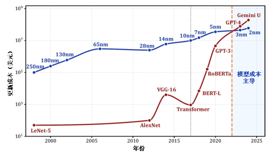
Thus, the value of a processor lies not in how many programs it can support or how many model generations it can survive, but in whether it has found a task with sufficiently high value—even if it is just one task. Today, historical conditions have quietly changed. Humanity has obtained the first neural network truly worth hardwiring: ChatGPT. The application value created by LLMs needs no further elaboration, but we can quantify it intuitively: a dedicated cryptocurrency miner earns less than one cent per second; whereas, at current pricing, a single Hardwired LPU node could generate revenue of up to 20 CNY per second.
Even so, there will always be skeptics: “LLMs iterate so fast. What if the algorithm changes to Mamba tomorrow? Are you going to replace the hardware?”
Why not? In the past, computers emphasized software updates because the marginal cost of software iteration was essentially zero. But today, the capital investment required to train a competitive LLM has historically surpassed the cost of mask revisions for advanced process chips. Under these conditions, the model—being more expensive—is the enterprise’s core asset, while the chip, relative to the model, has become a “consumable.” If the application value of an LLM is sufficient to drive companies to release new models quarterly or even monthly, then retiring a batch of custom processors along with the old model results in negligible economic loss. Compared to the fractional extra cost of discarding chips, the benefits brought by specialized hardware are transformative. One Hardwired LPU node can replace a GPU cluster composed of approximately 2,000 H100s. Due to the drastic reduction in the number of chips required, data center construction, operations, electricity, and embodied carbon emissions can be reduced by hundreds or thousands of times. Facing the disorderly growth of inference demand, manufacturing “monthly disposable” hardware and achieving model updates through physical replacement will inevitably become a more economical and environmentally friendly choice.
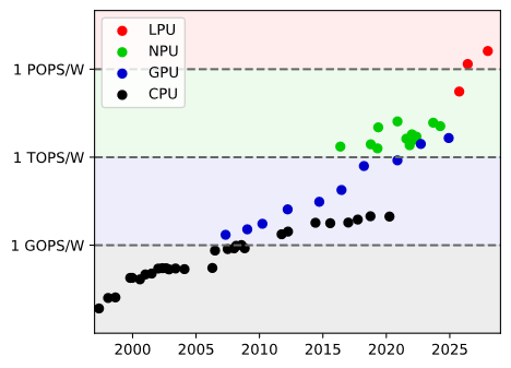
In our view, although it is technically implemented in the most immutable way, the Hardwired LPU is still a General-purpose processor. It implements an LLM of general utility, so the hardware automatically inherits general utility. It implements token processing directly at the hardware level, where instructions and data are input as prompts to program general problems. Its software-hardware interface (ISA) is natural language, which cannot be exclusively monopolized by any single company, nor does it require the assistance of software like CUDA, naturally eliminating the problem of ecosystem monopoly. Its computational energy efficiency can reach the 1 POPS/W level, forming the fourth paradigm of general-purpose processors (Token, POPS/W) following CPU (Scalar, MOPS/W), GPU (Vector, GOPS/W), and NPU (Matrix, TOPS/W).
While the original concept existed, the technical solution was not easily achieved in a short time. For those without long-term persistence in exploration, the idea sounded overly impractical until the entire path was mapped out. Consequently, since the birth of ChatGPT, individuals and companies have constantly proposed similar ideas, only to abandon them quickly. To our knowledge, UIUC, ARM, UMich, and the University of Tokyo are working on similar technologies but have not reached a level capable of supporting LLMs. Startups like Etched and Taalas have publicly announced plans to launch similar products but have not yet succeeded. Our team began researching reasonable technical solutions for realizing Hardwired LPUs in March 2023. By traversing multiple research fields—algorithms, architecture, and process technology—and organically combining two key innovations, we finally reduced the estimated cost to a reasonable range:
- Hardwired-Neurons (HN) Architecture: Through a mathematical transformation (which the team calls Primitivization), model weight information is extracted from the 2D planar device array and expressed instead by the topological structure of metal wires in 3D space. Each weight only needs to be encoded as a connection relation of a metal wire. This method utilizes a resource in architectural design that is usually only considered during physical design—the vertical space of metal wiring in the chip’s back-end-of-line (BEOL) process—achieving an approximate 15x increase in encoding density.
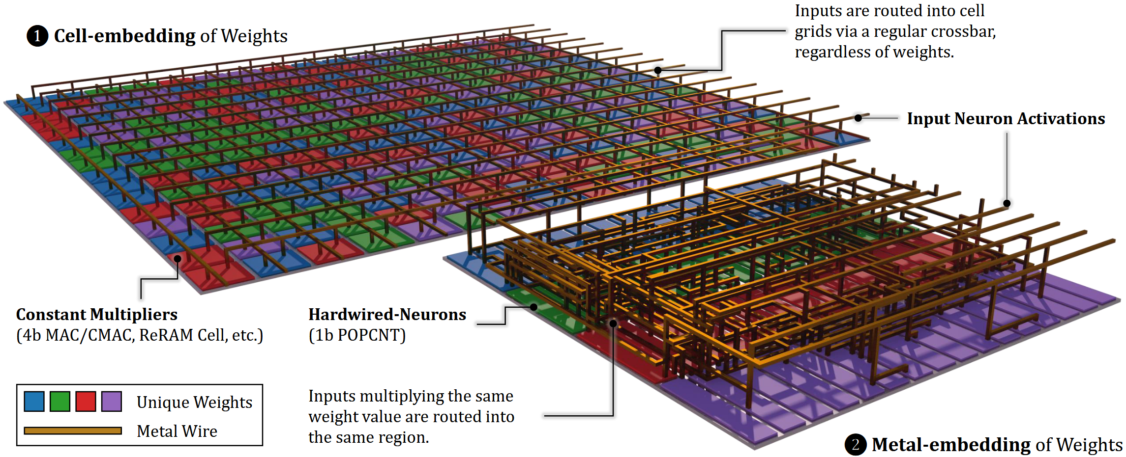
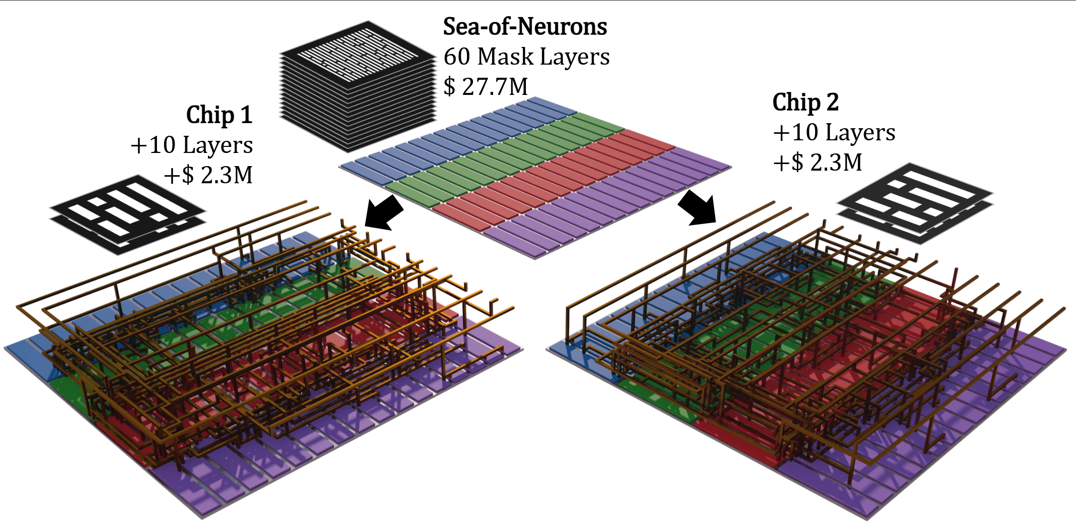
- Sea-of-Neurons (SoN) Design Methodology: Following HN’s expression of model weights as metal wires, we further constrained the circuit structures related to model weights to only the M8-M11 metal layers. This means that out of the 70 mask layers required for each chip, 60 layers can be reused across different models. SoN reduces the mask costs for the first tape-out and subsequent revisions by 86% and 92% respectively, making chip customization for specific models economically attractive.
The academic prototype system “HNLPU” has been verified through post-layout simulation. Under the conditions of a 5 nm process and an area of 16×827 mm², it fully implements the OpenAI open-source model GPT-OSS 120B, maintaining the model’s native FP4 numerical precision. In a single-card comparison, its performance and energy efficiency reached 5,555 times and 1,047 times that of the Nvidia H100, respectively. In a large-scale deployment scenario with annual hardware updates, HNLPU offers advantages of 1,496x in operating costs (OpEx), 41.7x in total cost of ownership (TCO), and 357.2x in total carbon emissions compared to a GPU cluster.
The Hardwired LPU is a processor paradigm defined by the following: it possesses general, programmable devices (for calculating attention, positional encoding, activation, sampling, etc.), a memory hierarchy for storing key-value sequences, a high-speed interconnect system spanning multiple chips, and a massive constant matrix operation unit (the HN array). The common structure of the HN array is prefabricated by upstream companies. After downstream enterprises determine the LLM model weights and place an order, metallization is completed to write the weights, allowing for the rapid and low-cost production of ultra-efficient chips equipped with various models. We predict this new industrial model will replace the GPU’s monopoly in the long-term, large-scale inference deployment market, though it requires the strongest possible deep integration between model companies, chip design firms, and the semiconductor manufacturing supply chain. Although many challenges remain, the history of Structured ASICs and Gate Arrays (Intel still operates an eASIC business), which once held a place in the chip industry, proves that this path is inherently viable.
This year, we expect to continue releasing fine-tuning architecture schemes and new layout designs to achieve low-cost model fault tolerance and hot-patching, further reducing the revision cost of changing models by more than ten times. Simultaneously, we are actively advancing the trial production of proof-of-concept prototype systems. Supported by the National Key R&D Program, we are fabricating a hardwired human-computer interaction processor chip based on the HN structure using domestic process technology. It is expected to achieve a computational energy efficiency of no less than 1.5 POPS/W @ FP4. This chip is poised to become the world’s most energy-efficient standard CMOS digital logic chip.
We invite colleagues to follow our latest progress.
(This article contains excerpts from the draft of “Hardwired LPU: A New Processor Paradigm in the Era of Large Language Models.” Original authors: ZHAO Yongwei, HAO Yifan, LIU Yang, CHEN Yi, CHEN Yunji)